


.svg)
Investing in AttoTude: Reinventing Interconnects for the AI Infrastructure Era
Investing in AttoTude: Reinventing Interconnects for the AI Infrastructure Era
TGVP is excited to announce our investment in AttoTude, a semiconductor and connectivity technology company developing a new class of high-speed interconnects for AI and hyperscale data centers. Our investment thesis is based on a fundamental shift taking place in AI infrastructure: the bottleneck is moving from compute to connectivity.
The rapid scaling of AI models has driven extraordinary demand for GPUs, accelerators, and memory. But adding more processors alone does not create a more powerful AI system. Thousands—or increasingly tens of thousands—of processors must continuously exchange enormous amounts of data with extremely low latency. As AI systems scale, the network connecting these processors is becoming as important as the processors themselves.
Today, these connections are primarily served by two technologies: electrical interconnects over copper and optical interconnects over fiber.
Copper is relatively simple and economical, but it becomes increasingly challenging to maintain bandwidth, reach, and power efficiency as data rates rise. Optical communication provides much greater reach and bandwidth, but requires electrical-to-optical conversion and additional optical components, introducing cost, power consumption, and system complexity.
AttoTude is developing a fundamentally different approach.
ASICs over Dielectric : A New Path Between Copper and Optics
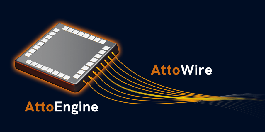
AttoTude has developed ASICs-over-Dielectric, an interconnect architecture that couples custom semiconductor ASICs directly to a low-loss dielectric transmission medium. Instead of converting electrical data into light, AttoTude moves extremely high-frequency electrical signals directly over dielectric material – closing the gap between traditional copper and optical interconnects without the cost and complexity of optical conversion. The company describes this architecture as “ASIC over Dielectric.”
AttoTude’s approach is designed to combine some of the most attractive characteristics of electrical and optical connectivity: the integration and manufacturing advantages of semiconductor electronics with the bandwidth and reach required by increasingly large AI systems. AttoTude has demonstrated its technology at data rates ranging from hundreds of gigabits per second per lane, and the architecture is designed to scale to 200, 400 and 800 Gb/s per lane. The company is targeting both scale-up networks, which connect accelerators into tightly coupled AI compute systems, and scale-out networks, which connect those systems across increasingly large data centers.
If successfully commercialized at scale, this could provide AI infrastructure designers with another fundamental option beyond the traditional choice between copper and optics.
Why This Matters for AI
AI infrastructure is increasingly becoming a communications problem. Training and inference workloads distribute computation across enormous numbers of accelerators. The value of those processors depends on how quickly and efficiently they can exchange data. Every additional conversion, switch, and interconnect adds power consumption, latency, cost, and potential points of failure.
AttoTude’s architecture is particularly compelling because it attempts to address several of these constraints simultaneously: bandwidth, power, reach, reliability, cost, and system complexity. Rather than incrementally improving today’s copper or optical architectures, AttoTude is introducing a new physical layer for moving data.
We believe innovations of this kind will become increasingly important as the AI industry moves from individual accelerator performance toward optimizing the performance of entire computing systems.
An Exceptional Team
Another important reason for our investment is the depth of AttoTude’s team. AttoTude was co-founded and is led by Dave Welch, PhD, one of the pioneers of modern optical communications.
Dave previously co-founded Infinera, where he helped pioneer photonic integrated circuits and build the company into a major optical networking provider. Earlier, he served as CTO and VP of Corporate Development at SDL, which ultimately merged with JDS Uniphase.
Over his career, Dave has received more than 200 patents, authored more than 300 publications, and was elected to the U.S. National Academy of Engineering. He is also a Fellow of both IEEE and Optica.
Building a completely new interconnect architecture requires deep expertise spanning semiconductor design, communications, materials, packaging, and large-scale networking. We believe AttoTude has assembled a team with the technical depth and industry experience required to pursue such an ambitious opportunity.
Strategic Relevance to TOPPAN
AttoTude’s new approach to connectivity creates exciting opportunities to explore potential connections with TOPPAN’s expertise across semiconductor packaging, manufacturing, and materials. We see particular potential to explore how our respective capabilities can help address connectivity challenges faced by customers, including the growing need for reliable, high-performance interconnects as AI infrastructure scales.
For TOPPAN, AttoTude also brings a fresh approach beyond conventional copper and optical technologies. We believe it is important to explore both the evolution of established technologies and new approaches like AttoTude’s, with the same goal: solving real challenges for our customers. Through TGVP’s investment, we are excited to support AttoTude as it brings this unique technology to market, while exploring how AttoTude and TOPPAN can create mutual value for customers.
Building the Connectivity Foundation for the Next Generation of AI
We believe the next generation of AI infrastructure will require innovation at every level of the computing stack—from processors and memory to packaging and networking.
As compute continues to scale, moving data may ultimately become as important as computing it. We are excited to partner with Dave Welch and the AttoTude team as they work to build a new connectivity foundation for the AI era.
About TGVP
TGVP is the U.S. Corporate Venture Capital arm of TOPPAN, Inc. Founded in 2022 and based in San Mateo, California, TGVP focuses on venture capital investments in U.S. startup companies in Sustainability and Digital Transformation. For more information, please visit www.tgvp.vc
About TOPPAN
Established in Tokyo in 1900, TOPPAN is a leading and diversified global provider committed to delivering sustainable, integrated solutions in fields including printing, communications, security, packaging, décor materials, electronics, and digital transformation. TOPPAN offers optimal solutions enabled by industry-leading expertise and technologies to address the diverse challenges of every business sector and society and contribute to the achievement of shared sustainability goals. For more information, please visit www.holdings.toppan.com/en/
About AttoTude
AttoTude is developing advanced interconnect technology for AI and hyperscale data center applications. Its AttoEngine and AttoWire technologies use wired THz communications to provide high-speed connectivity designed to improve bandwidth, power efficiency, reliability, reach, and scalability for next-generation AI infrastructure. AttoTude is headquartered in Menlo Park, California, with an additional office in Ottawa, Canada. For more information, please visit www.attotude.com.